Reverse Engineering the V86P PSU (Part 1)
My V86P did not come with a PSU - this makes things all sorts of interesting. Whilst 8.5V isn't hard to get from a bench supply, it's not a particularly common voltage for off the shelf PSUs, especially not at 4A (which is what the original unit is rated for). To top things off, I've suspected for a while that a good chunk of the NiCd charging circuitry is inside the PSU, rather than than the laptop itself, but precisely how much I didn't know. I started with a few simple tests with an ohmmeter between the various power input pins, and was able to confirm that two pins on the 6-pin PSU connector are connected to Gnd, two pins are connected together (I know from the actsirius1.co.uk site that these are the main 8.5V in), the pin immediately above these connects directly through to the positive pin of the NiCd battery pack, and the last pin is an unknown. The PSU connector is located on a separate PCB under the motherboard, inside a metal housing that makes up half of the battery compartment. A short cable protrudes from this housing which connects to a 6-pin header on the motherboard, and a pin just above the power switch. There's also a separate wire that goes to a ring loop which goes through one of the motherboard screws - presumably chassis ground.
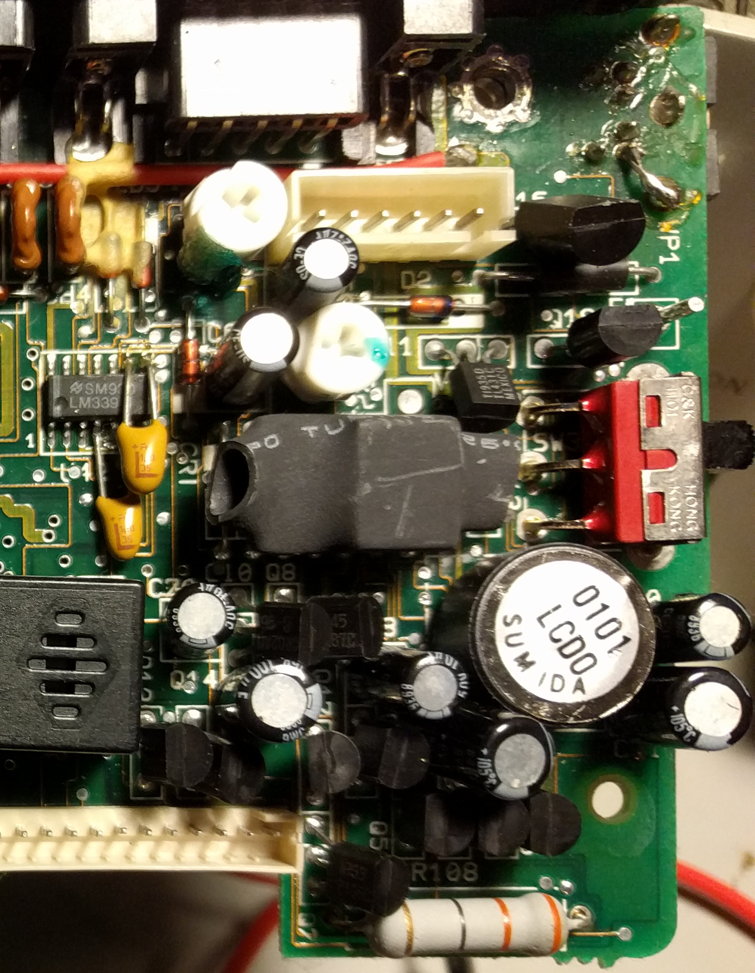
DC-DC converter section of Motherboard
You can see the 6-pin connector top-centre in the above image, and the separate pin just above the power switch on the right-hand side. The red wire runs across to the +ve terminal of the battery connector on the other side of the board, and provides additional current-carrying capacity (clearly the trace between the two endpoints wasn't sufficiently low resistance). Lifting out the metal housing reveals that the other end of this short cable splits into two - three conductors going to a TO-220 package attached to the metal housing (presumably an output transistor) and the other four going to a small PCB containing the power connector and a handful of components:
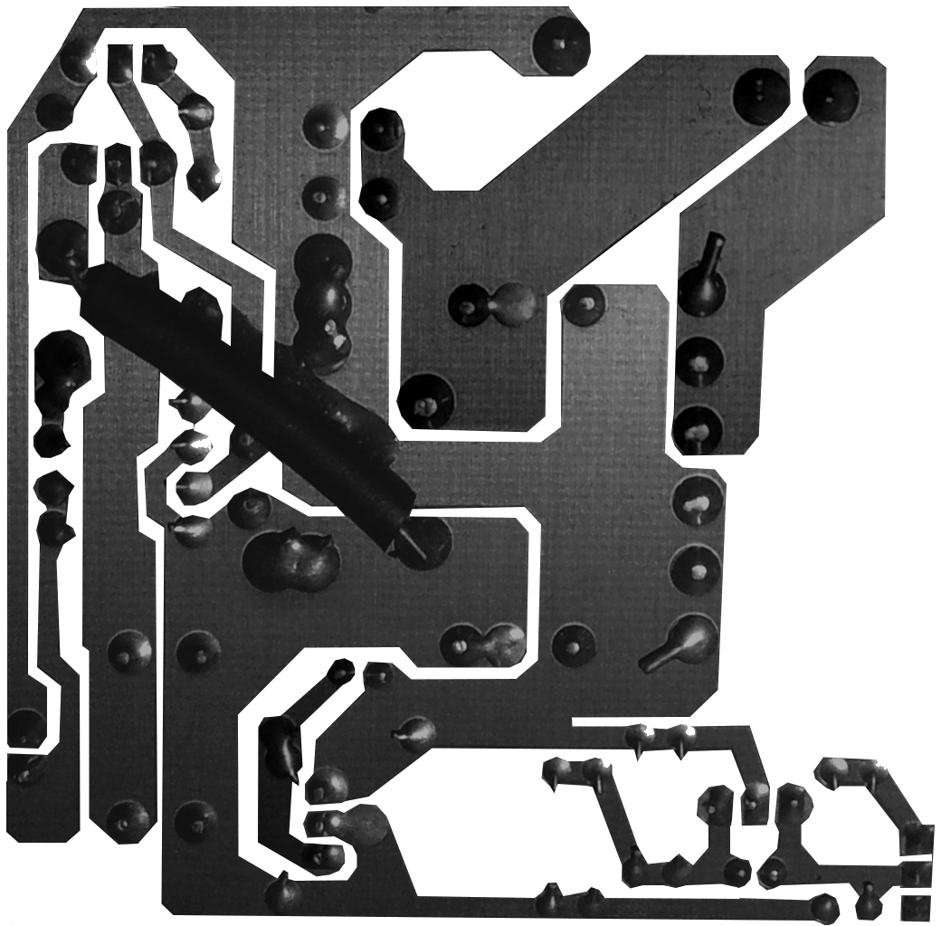
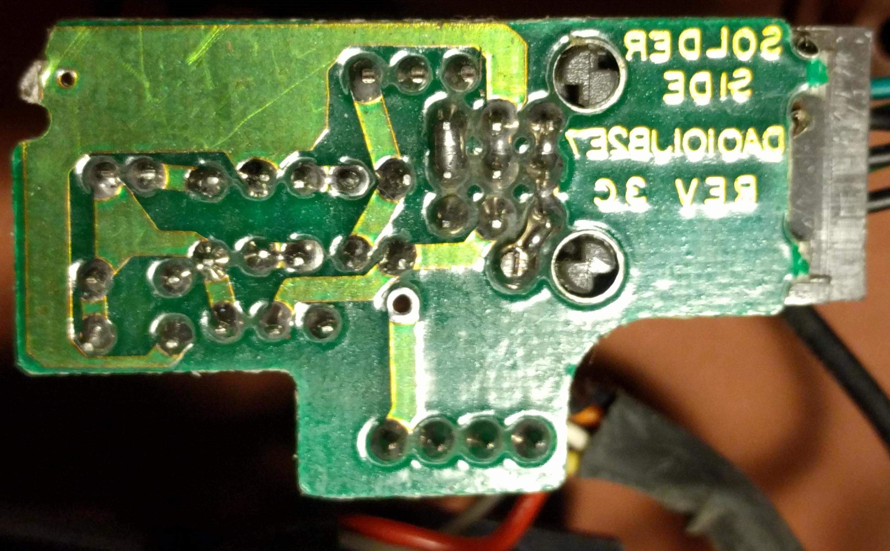
Power input board
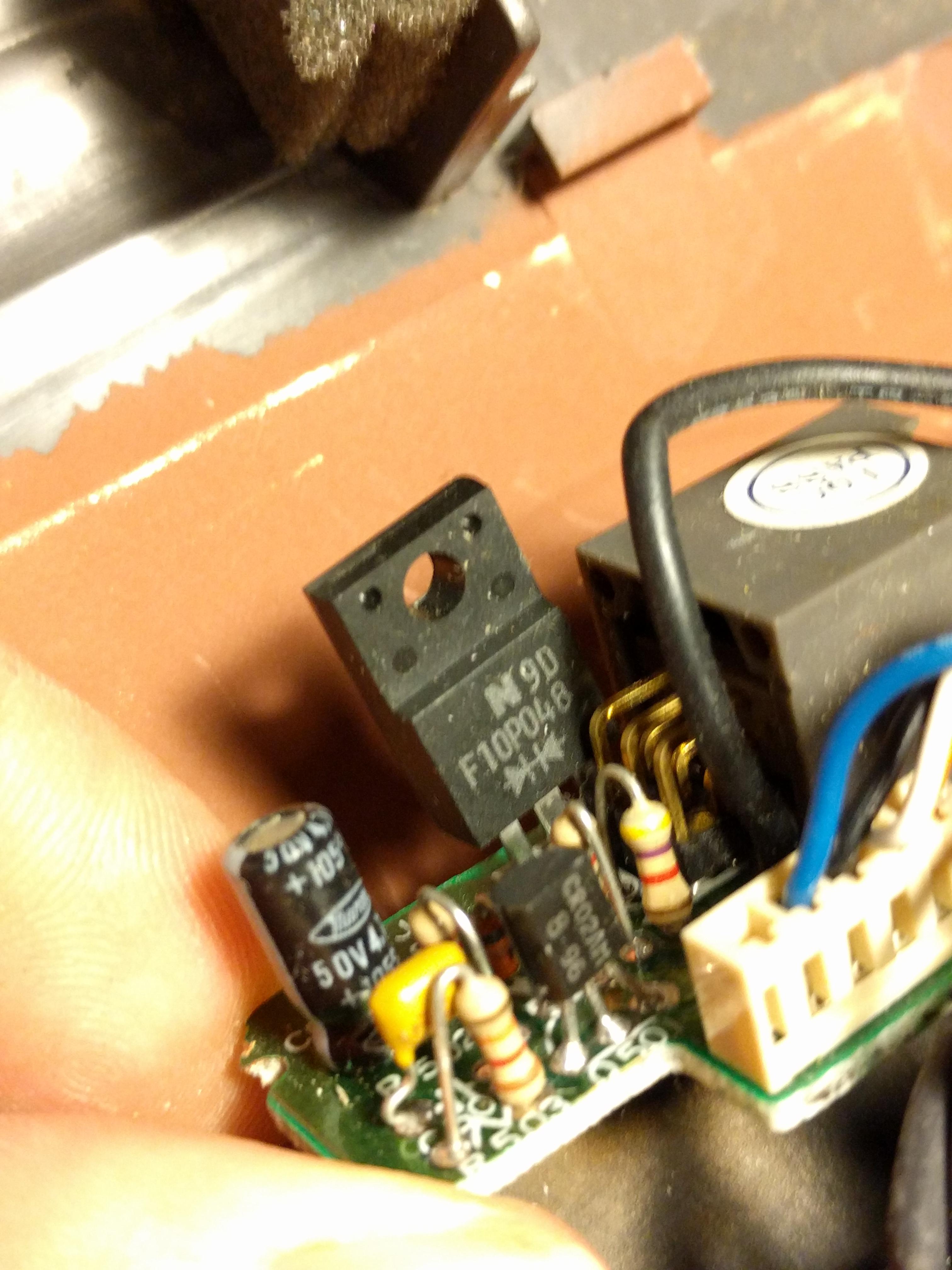
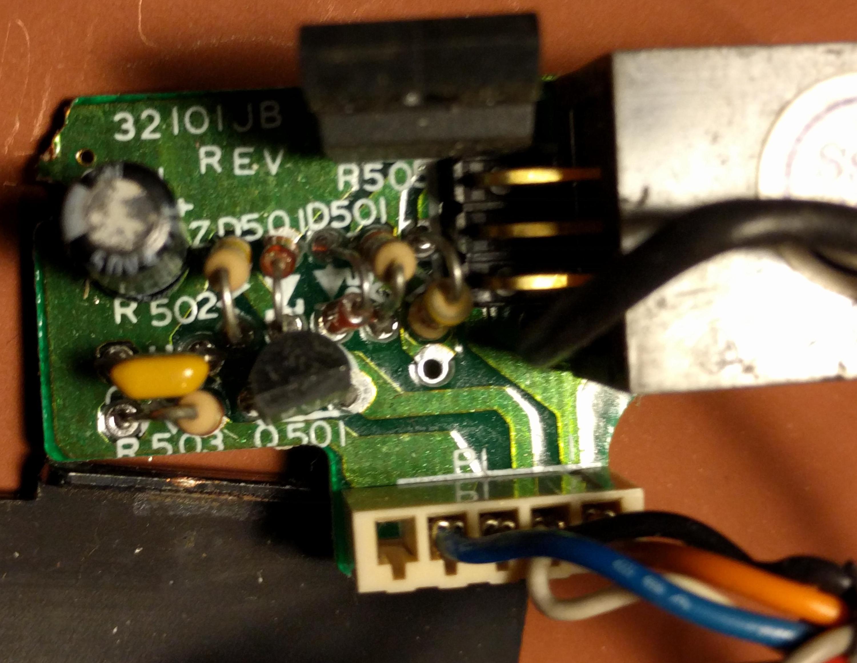
Looking at the components, the TO-220 is a dual-diode package and the TO-92 is an SCR/Thyristor. There's also a diode, a zener, a couple of caps, and a handful of resistors. For a simple board like this, it should be easy to reverse-engineer a schematic. As it's a double-sided board, the first step is to take photos of the top and bottom of the PCB:
Top side
Bottom side (reversed)
The bottom image has been mirrored - this essentially allows them to be super-imposed to make it a little easier mapping out the traces. From these images, I was able to place components onto a schematic, and draw in the connections between them. This is a bit of an iterative process: place components, add connections between them, move components around to make the diagram clearer, repeat. You start off with a schematic laid out similarly to the PCB, which isn't terribly neat (or clear), and slowly shuffle things around to make it more logical, until you end up with something you're happy with.

Power Input Board
From this, I was able to determine that the blue wire that goes off to the pin above the power connector (labelled Vin above) takes power from the (nominally 6V) battery and in the 8.5V input from the PSU. The battery +ve terminal passes straight through, as does Gnd. The mystery third line is almost certainly something to do with charging, but this board doesn't really help with identifying that. The next step was to try and do the same thing for the original PSU - but how to do that when I don't have one?
The solution came thanks to StickByDos on the vogons.org forums, who has both a functioning V86P and the matching PSU. He was able to pull the PSU apart and take some detailed photographs of the internals, along with making a few voltage measurements and confirming some component values. This was incredibly helpful - all the photos and notes he made can be found here. I was able to locate datasheets for all the semiconductors, which I've also linked from that page.
Rather than attempt to reverse engineer the entire board, and given it's clearly a switch-mode power supply, I decided to start with just the output section of the board. We know it's nominally 8.5V at 4A from the label on the PSU, so starting at the secondary winding of the output transformer, and the output side of the feedback optoisolator and then working toward the output to the laptop should give enough information. It's only a single-sided PCB, so tracing out component connections is easy - I started by isolating just the output end of the PCB in an image editor, mirroring it so it matches the component side when placed side by side, and then desaturating the image and removing the areas of the board not containing copper. The result is a nice high-contrast image of the output section of the PCB:

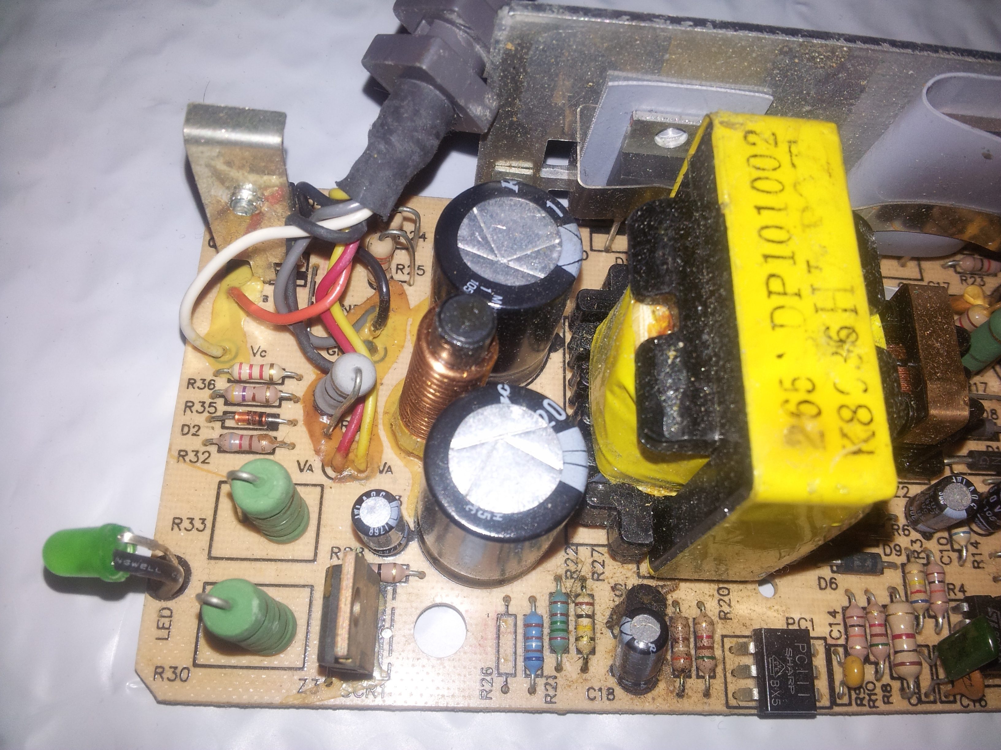
By comparing this to the top-side views of the board, it's a fairly straightforward process to reverse engineer the schematic, the end result of which is available here as a PDF.

My electronics skills here begin to let me down, but luckily I have friends who are more skilled. Without knowing what the Vchg signal does during a battery charge cycle, it's hard to determine precisely how things function. However, the current working hypothesis from someone who knows more than me is that when power is applied to the circuit, Va goes up, turns on Q501 through D501. Q501 turns off Q4, turning on Q3, charging the battery. If Vchg rises as the battery voltage rises, when this reaches the normal bias point of Vc (7.35V), Q501 shuts off, and the charger shuts off.
I've been able to identify currently available equivalents for the components in the output circuit, and a beefy 8.5V PSU is apparently not too hard to find, as the slim version of the PlayStation 2 console used an external 8.5V PSU. I think my next step here might be to put together a replica of the output circuit taking 8.5V in and generating the necessary Va, Vb, and Vc lines for the V86P.
February 4th, 2021 - 23:40
Ok, so JACKPOT — I have the factory schematics (!) for this machine. At some point, Victor was contracted by Stone Co in China, and the Chinese version of this machine is called Stone MS-1300 Chinese Typewriter. I happened to have the original service manual for that, which includes all original schematics.
https://software-archive.tifan.la/Stone-Chinese-TypeWriter/eBook/
Two files — 四通打字机电原理图.pdf schematics, 四通打字机原理与维修-610p.pdf service manual
Both are in Chinese, and they’re scanned books (bought from a used book store and asked someone in China to scan it for me). The last section of both books are about MS-1300 / V86p.
Hope that helps.