Upgrading the V86P HDD Controller
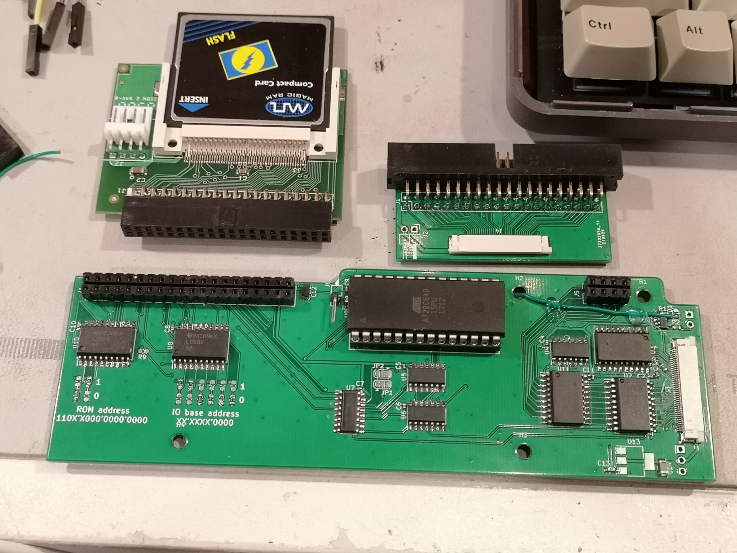
Back in a previous post I set about reverse engineering the HDD controller, and one of the things I was able to work out was the pinout of the connections to the mainboard. In fact, I commented that this looked like a stripped-down ISA bus with only the necessary signals being routed through - a fact confirmed by the system interface IC on the controller. I think I mused at the time at the possibility of fabricating a board that fits where the existing controller goes, but contains an XT-IDE (for those unfamiliar, this is an open-source IDE controller for 8-bit ISA systems that allows the use of regular IDE/PATA drives). In my last post, I documented my work with the expansion bus and testing with a regular 8-bit ISA XT-IDE card - which worked perfectly, with the exception that the top 384k of RAM (normally available via EMS) has to be disabled because there were conflicts with the default ROM location of the XT-IDE's BIOS. Pulling the internal controller and relocating the ROM location should address this.
Recreating the V86P Floppy Drive Riser
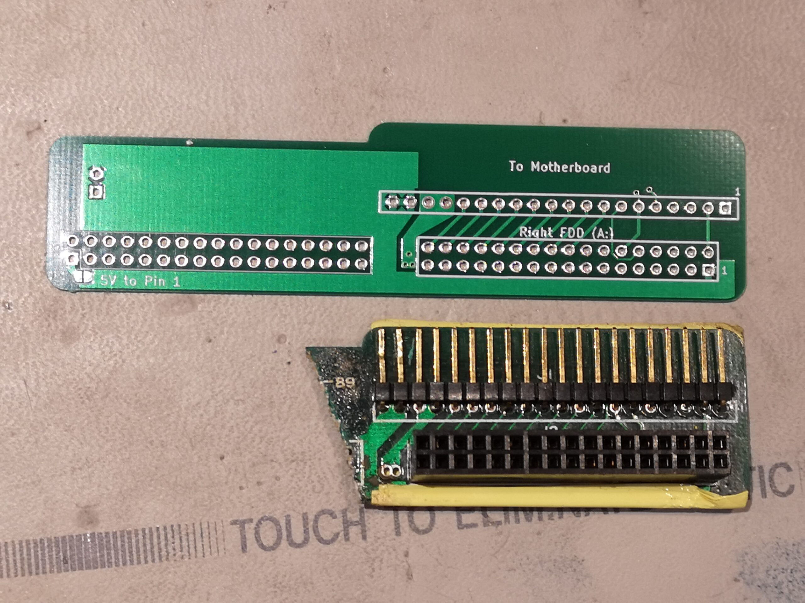
One of the things I remember from my original V86P back in the 90s is the way the floppy drives connected to the motherboard. The two drives were mounted back to back, with a riser card between them that connected to a socket on the bottom of the motsherboard. One of the things that would happen after a while is that one of the drives would rattle slightly loose and become disconnected - and thus stop working. The quick fix was to put a disk in both left and right drives and push inward on both disks at the same time - thus reseating the drives back on the riser card. Looking back, and comparing to my current system, I suspect my original system might have been missing one or two of the studs screwed onto the side of the floppy drive, securing it from lateral movement by engaging in holes in the metal battery enclosure.
Working on the V86P expansion bus
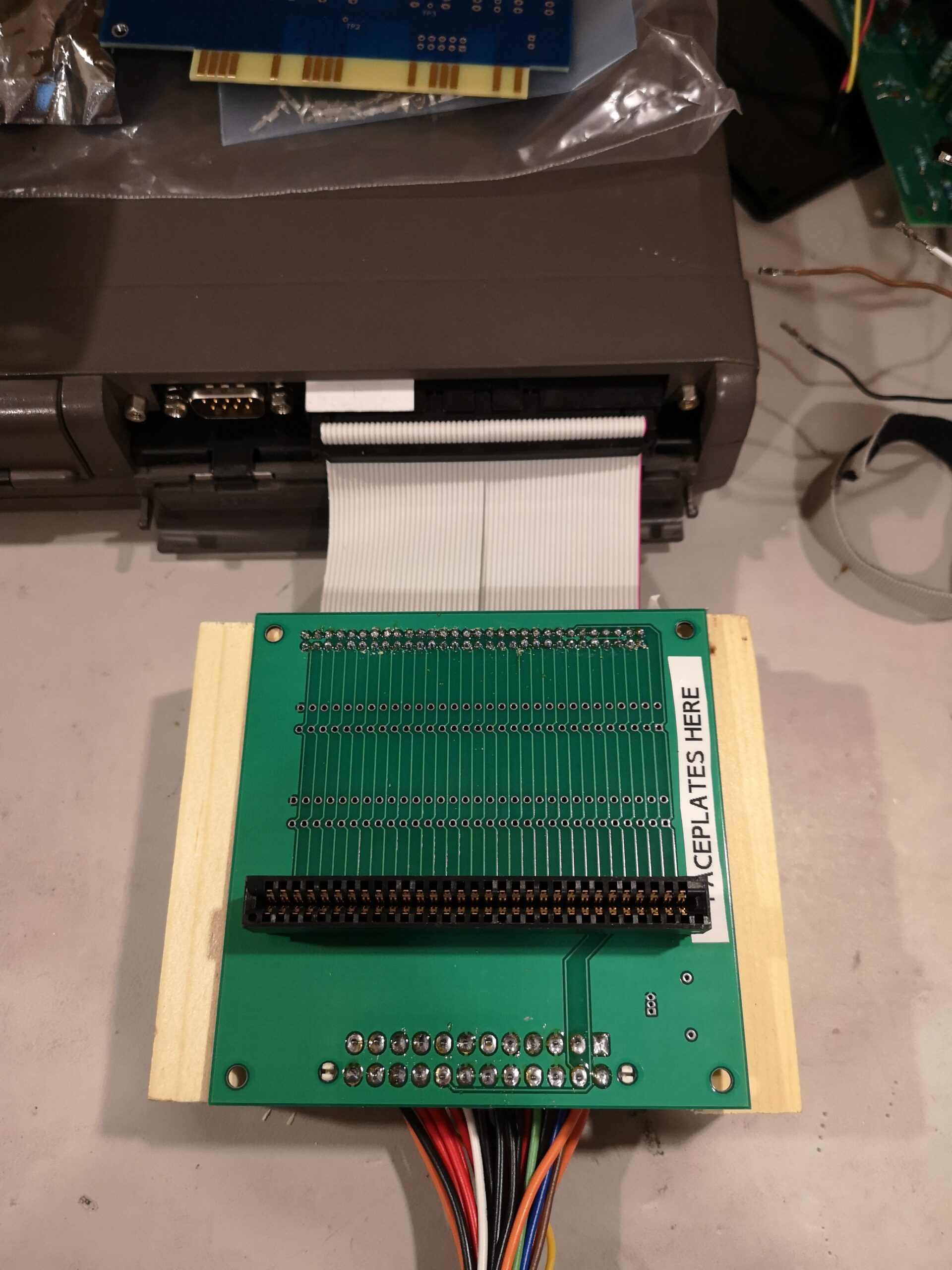
If you remember from this post, I'd previously reverse engineered the expansion interface pinout on the back of my V86P laptop and determined that it looked just like an ISA bus, but with the voltage rails removed (and replaced by grounds), with one exception that was connected to the 5V rail via a pull-up resistor. I'd mused at the possibility of building a board to let you hook up a regular ISA card - and that's exactly what I decided to do. Part of the motivation was to try connecting up an XT-IDE to hook up a more modern hard disk, thus allowing me to make a backup of the existing drive, and also to make it easier transferring data onto the laptop. What's more, once I'd confirmed the XT-IDE worked without issues, I could set about potentially replacing the internal hard disk controller.
New V86P posts coming soon!
Yes, I know it's been a long time since I last posted anything. I've not has as much time as I'd like to work on retrocomputing projects, and when I have, I've definitely not had the time to write up blog posts about them.
Those of you who hang around on the same Discord servers or IRC channels as I do will have seen things as they progress - I've taken to snapping pictures as I go and chatting about projects as I'm working on them.
I've finally been able to take some time to start writing up all the various projects I've been doing with my V86P laptop, so hopefully there'll be a bunch of posts coming up soon talking about the following things:
- Building an ISA expansion backplane and testing an ISA XT-IDE
- Building an internal XT-IDE controller and mounting a CF reader
- Building an RS232 SLIP to WiFi NAT dongle for network access
- Converting the system from a NiCd pack to a Li-Ion pack (and building a new charger to match) - although this is still a bit of a work in progress
I'll try and get the new posts up online soon - they're mostly written, I just need to go digging through four years of photos to pull out the ones that need including.
The JVC 26-pin Interface – Part 3
Ok - so I should probably have written this post in May last year when it was all still fresh in my memory, except I never seemed to have time, then I forgot all about it, so here we are. In the intervening time, I've had a couple of folk contact me - some asking about progress because they too have these drives and are looking at either reading the disk or replacing it, but I also had a note from Oleksandr Kapitanenko over at PortaOne recommending DREM, which is a device that I was aware of thanks to the TRS-80 Trash Talk podcast. Apparently in the time between me originally looking at the device and the time I started posting on the subject, they've added support for the 26-pin bus. So if you're one of those people who have a system with this interface and a dead disk - that might be a solution for replacing the drive and I highly recommend getting in touch with them. I'm still interested in digging into the V86P's specific setup, so there will be more posts on the subject coming up.
If you've not read the previous posts recently, here's a quick recap of where I'd got to (and partly for my own benefit to wake up the appropriate neurons): I'd reverse engineered the interface to the point where I could confirm the pinout and signalling; I'd identified /SERVO_GATE was a sector index pulse; I'd identified the configuration from the datasheet indicating the on-disk layout of a sector; I'd been able to dump a sector with its ECC data via DOS; I'd confirmed the controller is using 2,7RLL encoding; and I'd successfully identified the start of the sector pre-amble and sector marker. This post is going to try and get written down what I did in the month following that last post.
V86P Expansion
Retrochallenge RC2017/04 might be over, but I'm going to try and keep moving on this project. I'd already started on the pinout for the internal connectors used by the hard disk controller, and finishing that off seemed like a fairly straightforward task. Having done that, the Expansion Bus header on the back of the system was just a matter of following the same process.
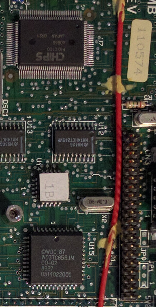
I started off with the hard disk controller, a multimeter, and the datasheet for the OMTI 5090 IBM PC Bus Interface controller. The datasheet has the pinout for the IC, along with a table identifying which pins were for the system bus, and which were for the system interface. For each of the system interface pins, checked for continuity to each of the pins on the header connecting to the motherboard. This got most of the header identified, with just a few unlabelled pins. To get those, I basically did the same thing on the motherboard, except in this case identifying the signals was more difficult. On the motherboard, many of the signals need to be buffered (or in the case of address lines, latched). For that, Victor just used 74-series logic - 74HCT244 and 74HCT373 specifically, which is well documented. I traced the signals from the connector to the appropriate buffer output, looked up the input on the datasheet, then traced the input back to the main Chips & Tech 82C100. From there I could identify the signal.
Retrochallenge Roundup (and a quick JVC update)
Well, it's the final night of RetroChallenge, so it's time for a closing post. As I'd expected, I didn't get anywhere close completing my goals, with lack of time being the age-old excuse. However, it was still a very productive project and I plan to keep pressing on and making semi-regular posts. Hopefully I can keep the momentum going even through RC is over for another 6 months. Although I didn't get a wiki up and running to store the information I was gathering, it's all up on this blog - so that's a start as far as making it available is concerned.
Other key milestones:
- I hacked together a working PSU for the V86P - learning a lot about switch-mode PSUs in the process
- I reverse engineered the output stage of the original PSU, using photos and some measurements being taken remotely, and captured the result as a kicad schematic
- I'm most of the way through a PCB layout for the charging section of the PSU, which will provide all the necessary voltages to the V86P to run and charge the NiCd pack given only a sufficiently beefy 8.5V PSU. The missing piece is finding a case I like, then I need to tweak the board dimensions to fit
- II got the V86P running with both its internal HDD and FDD
- I found datasheets for most of the key ICs in the system
- I'm about half-way through mapping out the pinout of the hard disk controller to motherboard interface pinout
- I confirmed the pinout of the 26-pin JVC interface
- I identified the SHIP_READY and SERVO_GATE lines as signal that the heads were parked and a sector index respectively
- I identified that DOS sees a 4 head disk with 512 byte sectors, but the disk itself only has one head select line - possibly there's some logic for splitting 1k sectors into two logical heads - developing some basic C routines to call BIOS int13h
- I've confirmed I can read the ECC blocks from the data block via DOS int 13h calls, which should make reverse engineering the polynomial used by the controller relatively straightforward
- And lastly, which I'm going to cover below - I think I've finally confirmed the disk is storing 2,7 RLL encoded data
The JVC 26-pin Interface – Part 2
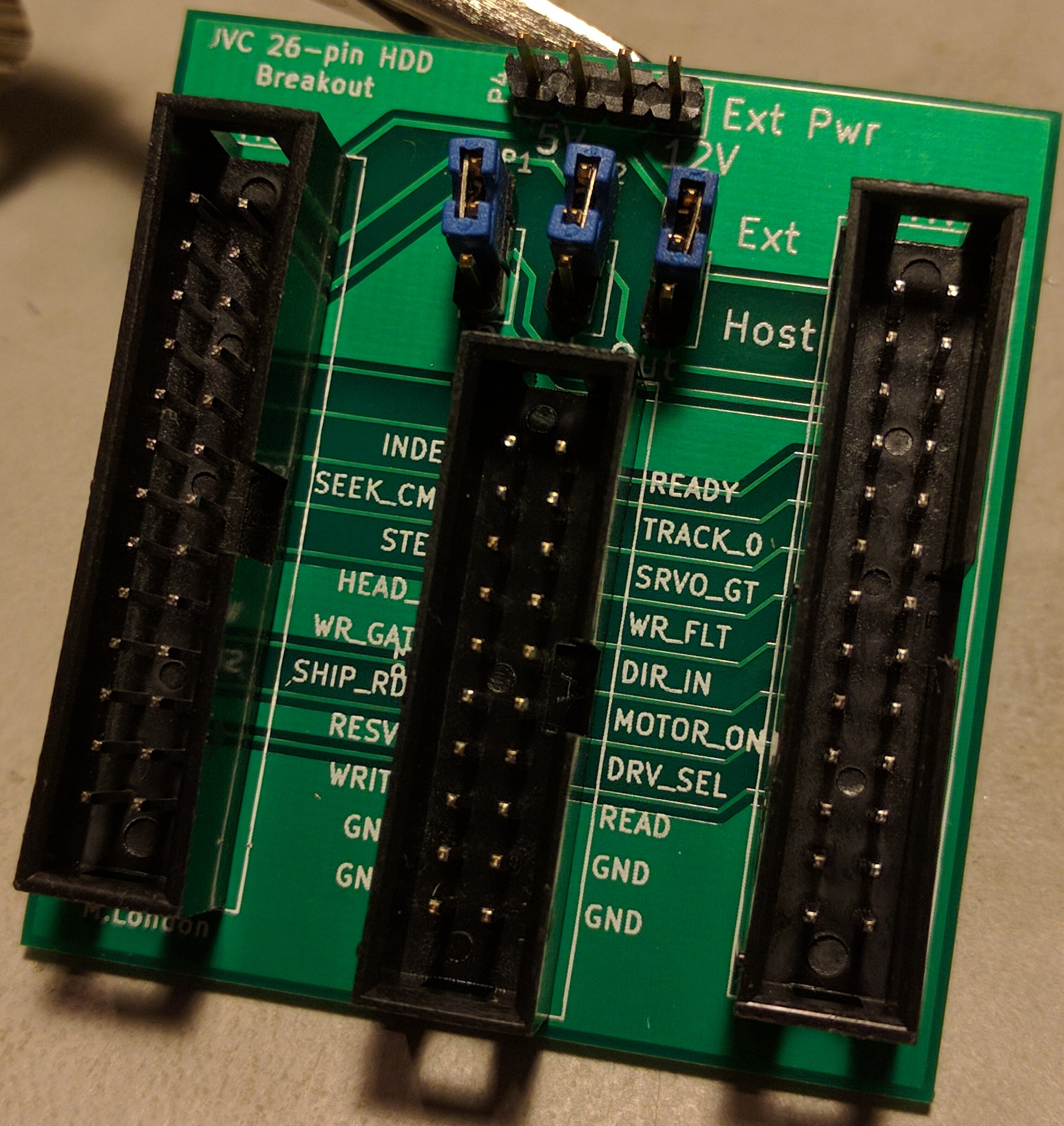
Welcome to the second part of my adventures with this slightly unusual hard disk interface. The more I dig, the more questions I raise - it's certainly good for raising the overall feeling of confusion. I think overall I'm making progress, but I'm still a long way away from even considering disk emulation (which was the original aim). As a quick recap of my previous posts - I designed a breakout board which brings the 16 lines of the 26-pin interface that aren't power or ground out to a pin header, along with support for supplying external power to the drive. I also got a power supply working so the laptop can run under its own steam, with both hard disk and floppy drive working correctly. I've got datasheets for most of the chips on the controller, and they look to be a standard ST506/412 RLL chipset, although with a few subtle differences and a mystery JVC chip - I've been reading through those and generally learning more about MFM than is probably necessary in 2017, but hey, isn't that what this hobby is all about?
Retrochallenge Half-Time Round-up
Well, I meant to write this up at the weekend, but that didn't happen. Better late than never - it's time for a half-time round-up, or perhaps a review of quite how much has been added on to my to-do list for this project. It really does seem to be one of those things where it appears complicated at first, then you get into it, and discover there's a significant number of smaller tasks you hadn't thought of to begin with. Despite the mamoth amount of work outstanding, it's actually been a pretty productive first half of the challenge, and I'm certainly enjoying it.
In which the author comes to grips with the SMPS
Power supplies are probably something we all take for granted. Pretty much everyone knows that if you plug an electronic device into the power outlet on the wall, there's a thing called a power supply that somehow converts the mains voltage to something lower (and safer). I suspect most people reading this post know at least a little more than that, maybe something about transformers. Perhaps like me, you're familiar with unregulated DC supplies (step down the AC voltage with a transformer, rectify it with some diodes, then smooth it with some big capacitors) and linear regulators (take an unregulated DC voltage and essentially dump the excess above the preset output voltage as heat), with a vague awareness that Switch Mode Power Supplies are far more common these days, and much more efficient.