The JVC 26-pin Interface – Part 3
Ok - so I should probably have written this post in May last year when it was all still fresh in my memory, except I never seemed to have time, then I forgot all about it, so here we are. In the intervening time, I've had a couple of folk contact me - some asking about progress because they too have these drives and are looking at either reading the disk or replacing it, but I also had a note from Oleksandr Kapitanenko over at PortaOne recommending DREM, which is a device that I was aware of thanks to the TRS-80 Trash Talk podcast. Apparently in the time between me originally looking at the device and the time I started posting on the subject, they've added support for the 26-pin bus. So if you're one of those people who have a system with this interface and a dead disk - that might be a solution for replacing the drive and I highly recommend getting in touch with them. I'm still interested in digging into the V86P's specific setup, so there will be more posts on the subject coming up.
If you've not read the previous posts recently, here's a quick recap of where I'd got to (and partly for my own benefit to wake up the appropriate neurons): I'd reverse engineered the interface to the point where I could confirm the pinout and signalling; I'd identified /SERVO_GATE was a sector index pulse; I'd identified the configuration from the datasheet indicating the on-disk layout of a sector; I'd been able to dump a sector with its ECC data via DOS; I'd confirmed the controller is using 2,7RLL encoding; and I'd successfully identified the start of the sector pre-amble and sector marker. This post is going to try and get written down what I did in the month following that last post.
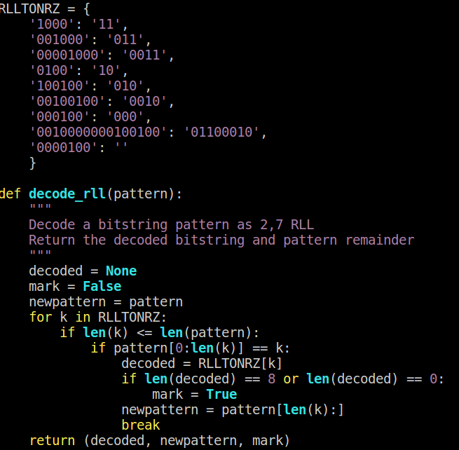
When I last left off, I'd mentioned that I'd just started to make progress on decoding some of the data coming from the drive. The datasheet for the OMTI 5027 indicates it's a 2,7RLL encoder/decoder - for those of you who have no idea what this means, hard disks don't store data as binary ones and zeros, they store data as magnetic flux transitions (i.e. flipping between N-S polarised and S-N polarised magnetic fields) , the same as other magnetic media like tape. You write data by charging the read/write head with an electric current, which in turn generates a magnetic field around it, which magnetises the area of disk surface immediately underneath it. Whether it's magnetised N-S or S-N depends on the polarity of the electric current flowing through the head. You read data by connecting the read/write head to the input of a sensitive amplifier and looking at the signal that comes out: when the head passes over a flux transition (i.e. the section of disk under the head changes from N-S to S-N or vice versa), you get a pulse of electric current from the head; and when there's no transition, you see nothing. There are several methods of encoding binary data as flux transitions, all of which result in a self-clocking data stream - this means that you don't need a separate clock signal to be encoded alongside the data in order to determine when the data line is at the next bit. I could go on to explain FM, MFM, and RLL encoding - but there's already a good write-up over on wikipedia, so I'll just point you there. For the sake of this post, I'll just include the 2,7RLL algorithm listed in the 5027 datasheet:
| Input NRZ Data | Encoded Data Out |
|---|---|
11 |
1000 |
011 |
001000 |
0011 |
00001000 |
10 |
0100 |
010 |
100100 |
0010 |
00100100 |
000 |
000100 |
You might be wondering about "NRZ" in the above table - that stands for Non-Return-t0-Zero, which means we're dealing with a signal that changes in polarity to represent 1 and 0, rather than presence and absence of a given current or voltage. As you can see (or read from the wikipedia article), 2,7RLL means that there is a minimum gap of two between flux transitions, and a maximum possible gap of seven (think a data stream of 00110011, which encodes as 0000100000001000).
The 5055 and 5027 datasheets indicated a value of 0x33 for the inter-sector gap, which translates to 00110011 - conveniently the example I gave above. That means that realistically, if we're looking at an inter-sector gap encoded as a series of multiple 0x33 bytes, we're going to see a pulse, then a gap for the count of seven, then another pulse, another gap of 7, etc. If we know the approximate timing (i.e. the expected data rate given a constant angular velocity in the drive), then we can use this series of pulses to feed a phase-locked-loop which can then provide the clock signal for decoding our data.
After the inter-sector gap comes a post-index gap, which is a user-programmable number of 0x33 bytes. This is followed by the ID Preamble, which is defined as a minimum of 12 bytes of 0xFF. This is 11111111 - that encodes to 1000100010001000. If we combine that with a couple of bytes of the previous 0x33, we get 00001000000010001000100010001000 - so we go from a gap of 7 between pulses to a gap of three between pulses. Next comes the ID Sync byte (also referred to as the Address Mark) - this is a modified encoding of 0x62 (10100010), which would typically be 0100010000100100, except that the datasheet indicates that "nrz 62 with a pulse one clock delayed", which is "an illegal combination that will never be used in a normal data field". Now, it doesn't actually specify which clock pulse gets delayed - so that's something to confirm. The datasheet contains a useful table that indicates the track format so we know what to expect:
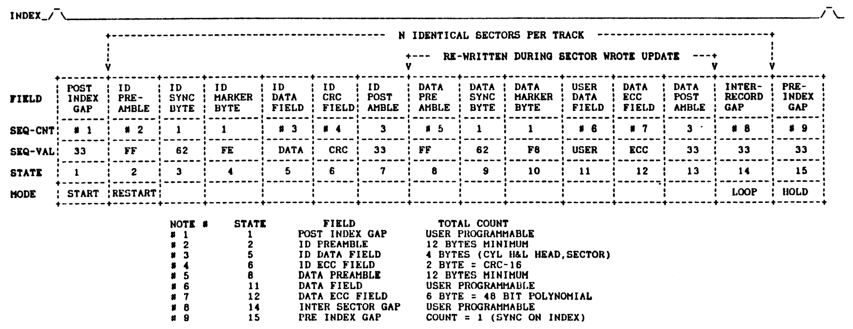
2,7RLL Track Layout
Looking at the timing from the logic analyser is one thing, but it's not going to be very easy to read out an entire sector that way. I did think about trying to write a protocol decoder, but I thought it would be easier to do a quick proof of concept in something quicker to start with and see how that goes. It's possible to export a CSV which gives relative timings since the start of the trace where the edges are, so we have a time for a pulse going high, and a time for it going low again. Importing this into a spreadsheet seemed like a good place to start: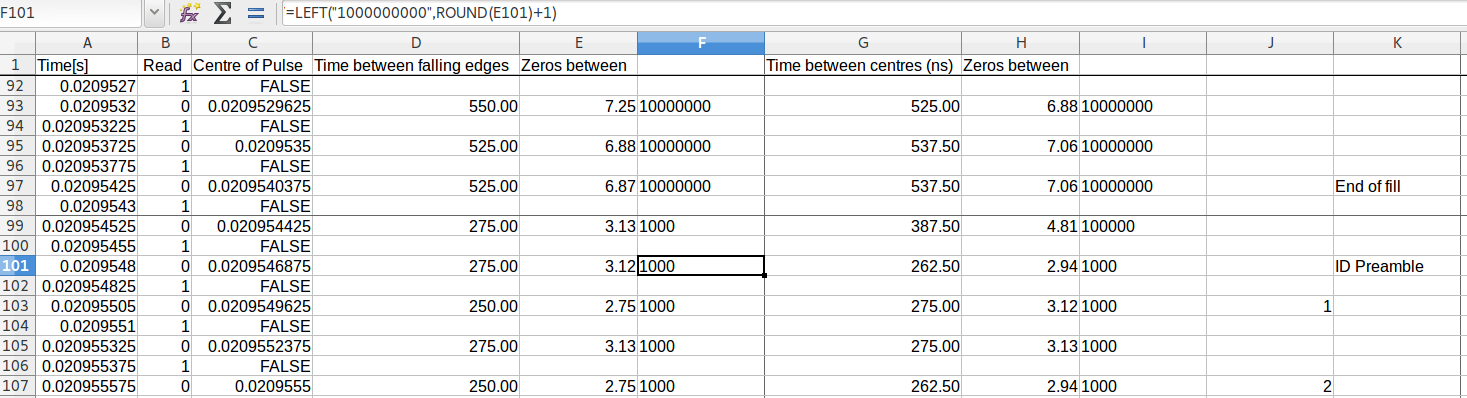
As you can see from the above image, the timings are a little wobbly - as you'll see later on - this is going to be a problem. I think it's a combination of signal integrity and logic analyser bandwidth - it's just not got the resolution to get the timings right. Once I started getting the 2,7RLL encoded values out of the spreadsheet, I started decoding them by hand, which did allow me to fudge the timings a little when I got an undecodable string in order to get something that seemed to work. As you can imagine, this was very time consuming, but once I'd got the feel for what was going on, I set about putting together a little python script that basically automated the process. I was able to identify the whole "delayed clock" thing in the address mark:
          6       2          f         8
          011    000    10   11   11   11   10
Expected: 001000 000100 0100 1000 1000 0100 000100
Observed: 001000 000010 0100 1000 1000 0100 000100
                     ^-- Delayed clock
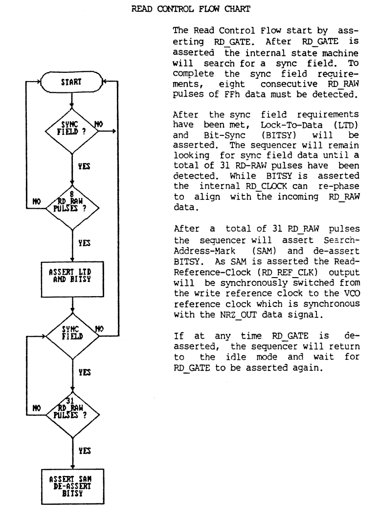
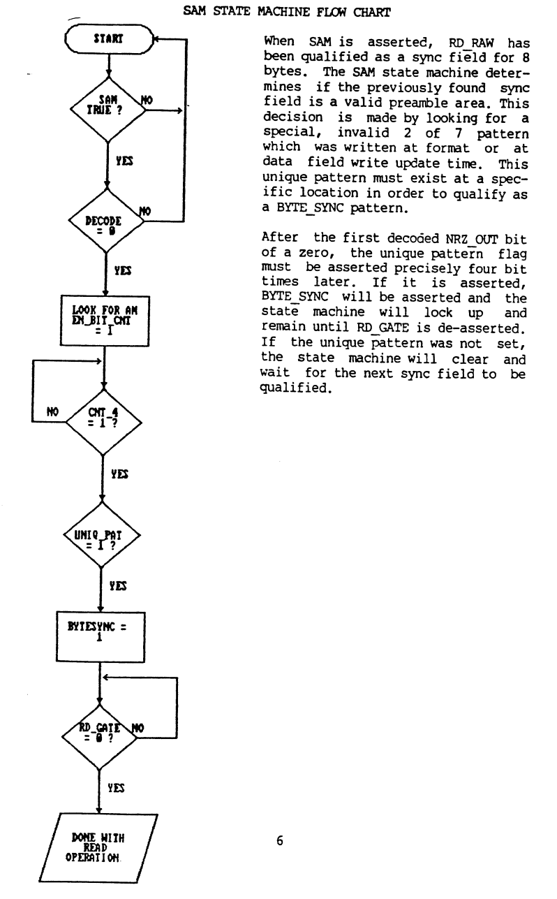
When it came to writing the python script, it was back to the datasheet, which contains two flow charts showing the read process and the sector address mark finding process:
I think at this point, I'll just link to the code and let you pick the bones out of that - I did try and make it fairly self-documenting.
The end result was... encouraging, yet disappointing. I was able to pick up the sector headers for most (but not all) sectors, but I wasn't able to get any sectors themselves decoded.
matt@henckels:~/v86p/rll/traces$ ./decode.py track0-head0.csv 2>/dev/null | head
00000000 fe 00 00 00 06 53 58 |.......|
Sector ID: 0/0/6
pattern too long: 575
00000000 33 33 33 ff |....|
00000000 fe 00 00 00 07 43 79 |.......|
Sector ID: 0/0/7
pattern too long: 54075
00000000 33 33 33 ff f4 3f ff ff ff ff ff ff ff ff ff ff |................|
00000010 ff ff ff ff fb 53 21 b1 b1 b1 b1 b1 b1 b1 b1 b1 |................|
00000020 b1 b1 b1 b1 b1 b1 b1 b1 b1 b1 b1 b1 b1 b1 b1 b1 |................|
matt@henckels:~/v86p/rll/traces$ ./decode.py track0-head0.csv 2>/dev/null | grep 'Sector ID' | sort -n -k3 -t/
Sector ID: 0/0/0
Sector ID: 0/0/2
Sector ID: 0/0/6
Sector ID: 0/0/7
Sector ID: 0/0/8
Sector ID: 0/0/10
Sector ID: 0/0/12
Sector ID: 0/0/14
Sector ID: 0/0/16
Sector ID: 0/0/18
Sector ID: 0/0/20
Sector ID: 0/0/21
Sector ID: 0/0/22
Sector ID: 0/0/24
Sector ID: 0/0/26
Sector ID: 0/0/28
Sector ID: 0/0/30
Sector ID: 0/0/31
Sector ID: 0/0/32
I did start looking into the ECC polynomial used for the sector data, but didn't get too far. Turns out it's not trivial to reverse engineer 🙂
So you might be wondering what's next, now I've apparently woken up again? Well, if you remember I was having some fun trying to get the V86P powered, and upon further diagnostics, the 5V rail kept collapsing even when powered from the nominal 6V battery supply. After looking at the board and talking to a few other like-minded folk who do more repair work than I, I figured replacing the handful of through-hole electrolytic caps that appeared to be part of a little switching power module on the right hand side of the board would be a good idea. I got the replacement caps and set about replacing the first - only to discover I'd bitten off a bit more than I could chew and my soldering skills weren't quite up to the job. A friend down in the US offered to recap the board for me as a favour (I'd previously sent him some gear I didn't need) - so I packaged up the board and sent it off to him. He successfully recapped the board and it now runs from his 6V bench supply without any problems, so hopefully that's solved that issue. Whilst it's down there, he's going to image the ROMs for me, including the two one-time programmable ROMs from the HDD controller board. One of these is probably the controller BIOS, and the other (potentially more interesting) is the firmware for the microcontroller that controls the OMTI 5055B Memory Controller and Programmable Data Sequencer. This little micro should be responsible for setting up sector layout, encoding, ECC, as well as the other control signals being sent to the drive. Whilst it might be possible to image the controller BIOS from the running system, it's not possible to get at the ROM for the micro on the controller, so dumping that may be somewhat enlightening.
If there's anyone out there who's looking for the V86P ROMs - I'm hoping to pass them along to bitsavers and archive.org for safekeeping.
I'll try and do another post once I get the ROM images and start investigating what the controller is up to. Stay tuned 🙂
May 26th, 2019 - 12:25
Have you made any progress with this? I have an Epson Equity LT laptop with a 20mb JD-3824LOYO drive. It is currently working, but I would be interested in building a solid state replacement for it.
May 29th, 2019 - 07:54
Not much of late – I’ve not had a lot of time to spend on the project lately. It’ll probably be a bit before I’m at a point to do more with the JVC interface – I’ve got an ISA backplane in the works, which should let me test an XT-IDE, and assuming that works, I plan to do an internal XT-IDE board that plugs in where the existing JVC controller goes, which will let me use a CF card for storage.
June 15th, 2019 - 02:17
I’m going to try to keep an eye out for this, thanks! The DREM is extremely interesting but kind of not idea for my application (at least 4 older mobile systems) as a substitute HD – and more than a little prohibitive pricewise. Probably quite worth the price, but the mobiles aren’t.
I am glad to find all this information about the pinouts and signals, it’s too bad there isn’t a RLL equivalent of CF cards’ IDE heritage that I know of – would simplify things.