V86P Expansion
Retrochallenge RC2017/04 might be over, but I'm going to try and keep moving on this project. I'd already started on the pinout for the internal connectors used by the hard disk controller, and finishing that off seemed like a fairly straightforward task. Having done that, the Expansion Bus header on the back of the system was just a matter of following the same process.
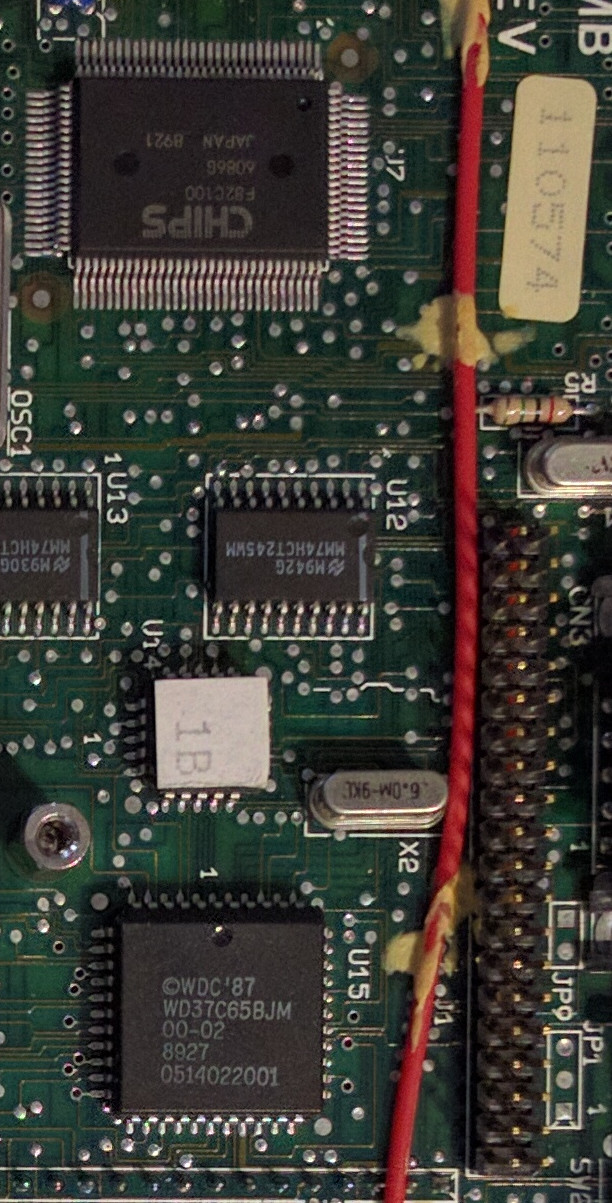
I started off with the hard disk controller, a multimeter, and the datasheet for the OMTI 5090 IBM PC Bus Interface controller. The datasheet has the pinout for the IC, along with a table identifying which pins were for the system bus, and which were for the system interface. For each of the system interface pins, checked for continuity to each of the pins on the header connecting to the motherboard. This got most of the header identified, with just a few unlabelled pins. To get those, I basically did the same thing on the motherboard, except in this case identifying the signals was more difficult. On the motherboard, many of the signals need to be buffered (or in the case of address lines, latched). For that, Victor just used 74-series logic - 74HCT244 and 74HCT373 specifically, which is well documented. I traced the signals from the connector to the appropriate buffer output, looked up the input on the datasheet, then traced the input back to the main Chips & Tech 82C100. From there I could identify the signal.
There are three headers of interest - two which connect to the motherboard, and another labelled TP1, presumably test points. After ringing out the connectors, the latter may actually be a jumper-block used during testing.
After getting the pinouts for the connectors to the HDD controller, I repeated the same process for the expansion bus connector - the results of which were pleasantly surprising. It turns out to be essentially the same pinout as a regular 8-bit ISA connector, but with a couple of differences. Firstly, the pins that would typically provide power rails are replaced with ground pins; pins A1 and B1 are not present, with /IO CH CHK is relocated to pin 13; and pin 7 is replaced with a 4.7k pull-up resistor to Vcc.
With all that said, here are the pinouts:
CN1 - to motherboard
| A_19 | 1 | 2 | A_18 |
| Gnd | 3 | 4 | Gnd |
| Vcc | 5 | 6 | Vcc |
| AEN | 7 | 8 | IRQ_5 |
| A_17 | 9 | 10 | A_16 |
| A_15 | 11 | 12 | A_14 |
| A_13 | 13 | 14 | A_12 |
| A_11 | 15 | 16 | A_10 |
| A_9 | 17 | 18 | A_8 |
| A_7 | 19 | 20 | A_6 |
| DRQ_3 | 21 | 22 | RSTIN |
| /DACK_3 | 23 | 24 | A_5 |
| /IORD | 25 | 26 | A_4 |
| /IOWR | 27 | 28 | A_3 |
| A_2 | 29 | 30 | A_0 |
| A_1 | 31 | 32 | Gnd |
| 33 | 34 | ||
| Vcc | 35 | 36 | Gnd |
| Gnd | 37 | 38 | Vcc |
| /MEMR | 39 | 40 | Gnd |
CN3 - to motherboard
| D_0 | 1 | 2 | D_1 |
| D_2 | 3 | 4 | D_3 |
| D_4 | 5 | 6 | D_5 |
| D_6 | 7 | 8 | D_7 |
TP1
| Gnd | 1 | 9 | DT_0 |
| Gnd | 2 | 10 | DT_1 |
| Gnd | 3 | 11 | DT_2 |
| Gnd | 4 | 12 | DT_3 |
| Gnd | 5 | 13 | /CNTA |
| Gnd | 6 | 14 | /CNTB |
| Gnd | 7 | 15 | /ROMDIS |
| Gnd | 8 | 16 | /RADR |
CN2 - to hard disk
| Gnd | 1 | 2 | /READ |
| Gnd | 3 | 4 | /WRITE |
| Gnd | 5 | 6 | Reserved |
| /SELECT | 7 | 8 | /SHIP_READY |
| Gnd | 9 | 10 | /WRITE_GATE |
| /MOTOR_ON | 11 | 12 | /HEAD_1 |
| /DIR_IN | 13 | 14 | /STEP |
| /WRITE_FAULT | 15 | 16 | /SEEK_COMPLETE |
| /SERVO_GATE | 17 | 18 | /INDEX |
| /TRACK_0 | 19 | 20 | /READY |
| Gnd | 21 | 22 | 5V |
| Gnd | 23 | 24 | 5V |
| Gnd | 25 | 26 | 12V |
Expansion Bus Connector
| RESET | 1 | 2 | D7 |
| Gnd | 3 | 4 | D6 |
| IRQ2 | 5 | 6 | D5 |
| Power On | 7 | 8 | D4 |
| DRQ2 | 9 | 10 | D3 |
| Gnd | 11 | 12 | D2 |
| /IO CH CHK | 13 | 14 | D1 |
| Gnd | 15 | 16 | D0 |
| Gnd | 17 | 18 | IO CH RDY |
| /SMEMW | 19 | 20 | AEN |
| /SMEMR | 21 | 22 | A19 |
| /IOWR | 23 | 24 | A18 |
| /IORD | 25 | 26 | A17 |
| /DACK3 | 27 | 28 | A16 |
| DRQ3 | 29 | 30 | A15 |
| /DACK1 | 31 | 32 | A14 |
| DRQ1 | 33 | 34 | A13 |
| /REFRESH | 35 | 36 | A12 |
| CLOCK | 37 | 38 | A11 |
| IRQ7 | 39 | 40 | A10 |
| IRQ6 | 41 | 42 | A9 |
| IRQ5 | 43 | 44 | A8 |
| IRQ4 | 45 | 46 | A7 |
| IRQ3 | 47 | 48 | A6 |
| /DACK2 | 49 | 50 | A5 |
| TC | 51 | 52 | A4 |
| ALE | 53 | 54 | A3 |
| Gnd | 55 | 56 | A2 |
| OSC | 57 | 58 | A1 |
| Gnd | 59 | 60 | A0 |
Italics indicate differences in pinout to the standard ISA pinout
Pin 7 appears to be a 4.7k pull-up to Vcc, presumably to indicate when the system is powered on
December 2nd, 2017 - 08:44
I’m very glad to see this post. I have two V86P, but they are OEM, so I need U16 and U17’s bin (BIOS). Can you send them to my mail box? thank you! 21631114@qq.com
December 2nd, 2017 - 13:59
Keep an eye on the blog – one of the things on my todo list is to dump all the ROMs, including the one from the HDD controller if I can
December 2nd, 2017 - 21:51
yes,I’m designing the main board of 82c100 and I like this。I also like to collect 82c100’s board。If you are interested, you can give me a mailbox address, and I’ll send you some design back.
December 2nd, 2017 - 21:53
I’m in China, I don’t know how to contact you
December 2nd, 2017 - 08:48
sorry, my English is very poor,I will be looking forward to your reply.
September 18th, 2020 - 01:42
Hi Mattinx,
I managed to attach an XTIDE to the V86P’s expansion port. Have a look here: https://twitter.com/hennichodernich/status/1306703430765993984?s=20
I plan to make a PCB for the internal HDD controller connector.
best regards
Henning
January 17th, 2022 - 17:55
wow, this is amazing! I have a Toshiba T1200 and would live something like that. right now the RLL HDD is dead of course, and an RLL drive emulator is very expensive.
were you able to make progmress on a PCB?